How does a FinFET work?
Who invented Gaafet?
Samsung has created its first 3nm GAAFET prototypes – Transistors beyond FinFET. By 2030, Samsung plans to become the world’s leading producer of semiconductors, overtaking the likes of TSMC and Intel to produce more of the world’s high-end silicon than any other company.
How FinFET reduces leakage current?
FinFET is suitable for future nanoscale memory circuits design due to its reduced short-channel effects (SCEs) and leakage current [6]. This technique provides increased operating speed by low-threshold MOSFET and reduced leakage by high-threshold voltage.
How FinFET reduces short channel effects?
Compared to a planar process in the same technology node, FinFET have reduced channel and gate leakage currents. The second gate can be used to control the threshold voltage of the device, thereby allowing fast switching on one side and reduced leakage currents when circuits are idle.
What is field effect transistor?
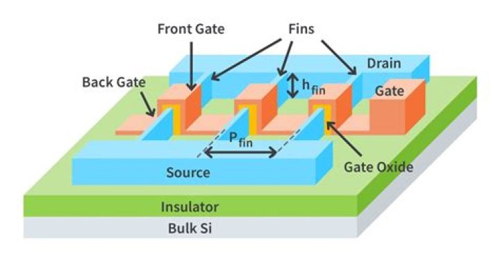
The field-effect transistor (FET) is a type of transistor that uses an electric field to control the flow of current in a semiconductor. FETs are devices with three terminals: source, gate, and drain. Field effect transistors generally display very high input impedance at low frequencies.
Is FinFET a CMOS technology?
The FinFET devices have significantly faster switching times and higher current density than planar CMOS (complementary metal-oxide-semiconductor) technology. FinFET is a type of non-planar transistor, or “3D” transistor. It is the basis for modern nanoelectronic semiconductor device fabrication.
How many gates does FinFET have?
In 2011, Rice University researchers Masoud Rostami and Kartik Mohanram demonstrated that FinFETs can have two electrically independent gates, which gives circuit designers more flexibility to design with efficient, low-power gates.
What is Nanosheet technology?
A nanosheet is a two-dimensional nanostructure with thickness in a scale ranging from 1 to 100 nm. A typical example of a nanosheet is graphene, the thinnest two-dimensional material (0.34 nm) in the world. It consists of a single layer of carbon atoms with hexagonal lattices.
How does FinFET reduce power consumption?
The lower operating voltage of FinFET devices results in up to 50% dynamic power savings. The advantages can be summarized as better technology parameters that give lower leakage and dynamic power consimption. In planar technologies this was done by changing the width of the device.
What is gate leakage current?
Leakage Current Due to Gate-Induced Drain Lowering (GIDL) When there is a negative voltage at the gate terminal, positive charges accumulate just at the oxide-substrate interface. Due to the accumulated holes at the substrate, the surface behaves as a p-region more heavily doped than the substrate.
How does the tri gate wizard card work?
This card gains these effects based on the number of monsters co-linked to this card. ● 1+: If a monster co-linked to this card battles your opponent’s monster, any battle damage it inflicts to your opponent is doubled. ● 2+: Once per turn: You can target 1 card on the field; banish it.
Why are tri gate transistors used in computers?
In 2011, Intel demonstrated tri-gate transistors, where the gate surrounds the channel on three sides, allowing for increased energy efficiency and lower gate delay—and thus greater performance—over planar transistors.
What’s the difference between FinFET and tri gate?
In current usage the term FinFET has a less precise definition. Among microprocessor manufacturers, AMD, IBM, and Freescale describe their double-gate development efforts as FinFET development, whereas Intel avoids using the term when describing their closely related tri-gate architecture.
What is the schematic symbol for dual gate MOSFET?
A dual-gate MOSFET and schematic symbol. A multigate device, multi-gate MOSFET or multi-gate field-effect transistor (MuGFET) refers to a MOSFET (metal–oxide–semiconductor field-effect transistor) that incorporates more than one gate into a single device.